Smart Watch
Capstone projects are a common rite of passage for engineering students. They show that four years of education can indeed manifest into real world contributions. Capstone's look different for each department and university, but they share common features. They are typically a semester or year long project that is designed to utilize the skills and knowledge of the student's major. Mechanical engineers typically design a system or mechanism, chemical engineers design a plant, and so on.
Going into Capstone I was excited, but also a bit nervous. Despite spending the last four years in school for engineering, you always have the fear of not being able to deliver. Our professor, a seasoned veteran of teaching capstone courses, impressed upon us our responsibility to not bore him. Many projects were suggested by our cohort. Some notable ones include:
- Navigation aids using computer vision
- Gamified Cup Pong
- Workout related apps
- Labo-labs style circuit learning tool
- Trash cleaning robot
Research
The first step to any project is research. Reading though material helps us get a sense of what is possible, what already exists, and what our options are. At this point in the project, we only have the vaugest idea of what our product would look like, so reading material helps to develop a basic intution of what's possible.
We would meet several times over the next few weeks as we began to hone in on what our project would look like. Since our professor set strict requirments on the novelty of our approach, we couldn't just use GPS like many (all) similar systems do. In our hunt however, we read about a technology called UWB (ultrawide band) that was used in devices like the iphone and airtag. Looking into it more, we found research where UWB was used to position moving drones and even to guide docking manuevers in space. UWB, it seemed, would be our ticket to accurately position users relative to each other. UWB is chosen for its unique benefits. The wide bandwidth allows for very accurate and percise time of flight measurements. Additionally, short pulses allow for better multipath rejection (the ability to ignore reflected signals) which is a common issue in indoor environments.
However there was a downside. Typical systems that take advantage of UWB for tracking use a split setup. Moving units, those are the ones being tracked, broadcast a UWB signal regularly. Tracking units are placed in fixed locations and use their known locations to determine the unknown location of the moving units. However in our version we would need each unit to act as a tracking and moving unit simultaneously. PDOA (phase difference of arrival) offered a solution. PDOA works by giving each unit two antennas that are spaced a percise distance apart. The implementation isn't unheard of, but UWB with it's high frequency, allows us to space them only millimeters apart which is essential for making a device that can comfortably fit on someone's wrist.
However no market solutions exist for this technology. What we did find was some research on using the system in a minimally sized tracker which we could base our own design after.
Design
Our design started by laying out all our requirments. Similar to how we would build software, we laid out user stories and built specific features with those in mind. Slowly the device began to take shape.
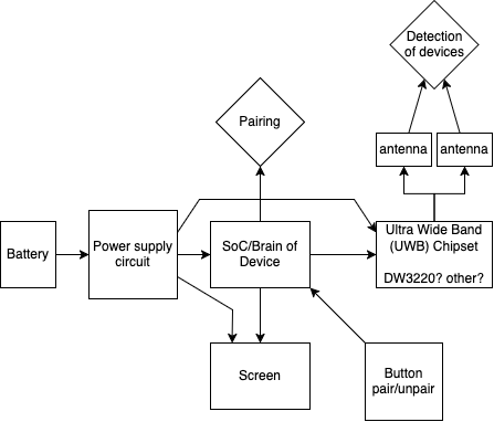
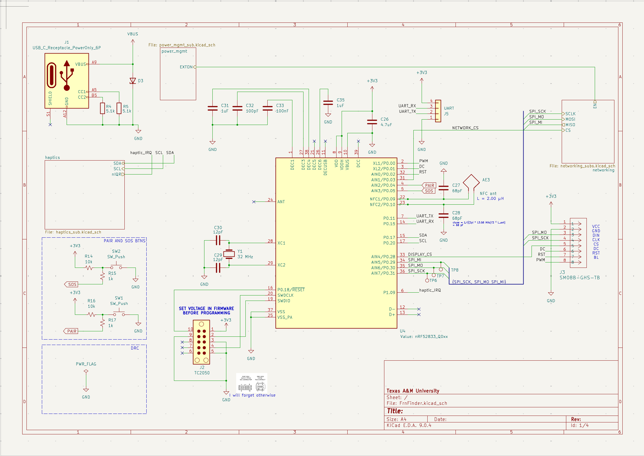
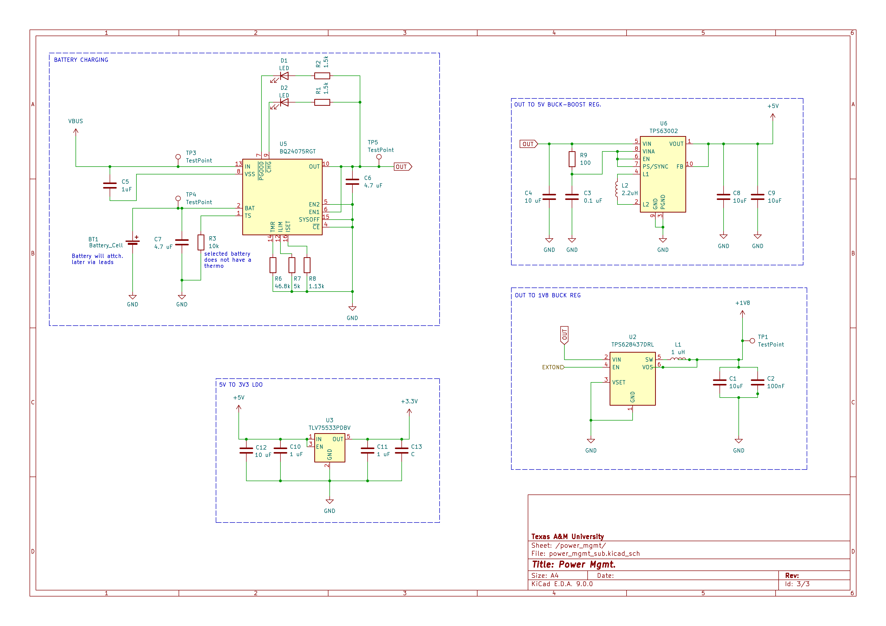
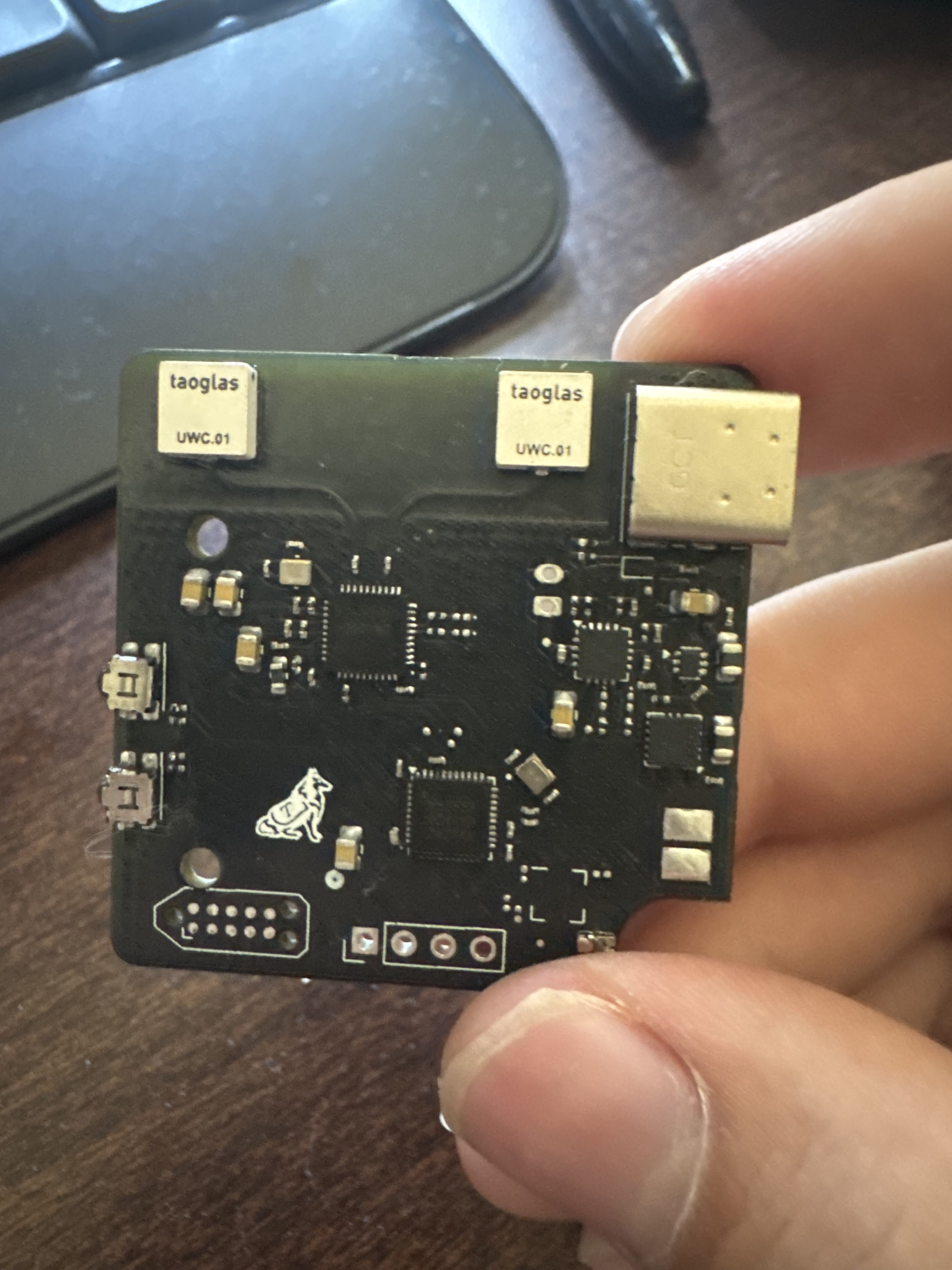
Building the design first takes place in schematics. We opted to use kicad due to its lower barrier of entry and crossplatform support. If we had longer than a semseter I believe altium would have been an equally good choice. We seperated into pairs in order to design the power, haptics, communication, and the interconnections via the SoC (system on a chip)
PCB Design
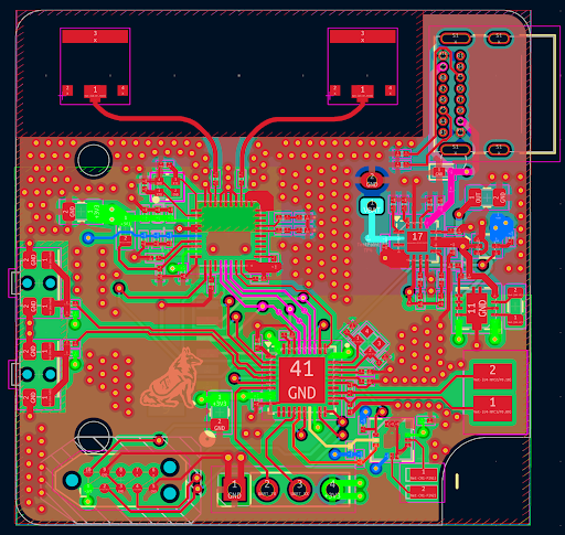
Converting the schematics to a 40x40mm pcb was a difficult task. As the only one with any experience in this field I did this singlehandedly over around a month. Our board ended up being over 100 components, across a four layer board. PCB design involves routing each trace--the thin copper wires embedded in the board--and placing components in logical, low interference positions.
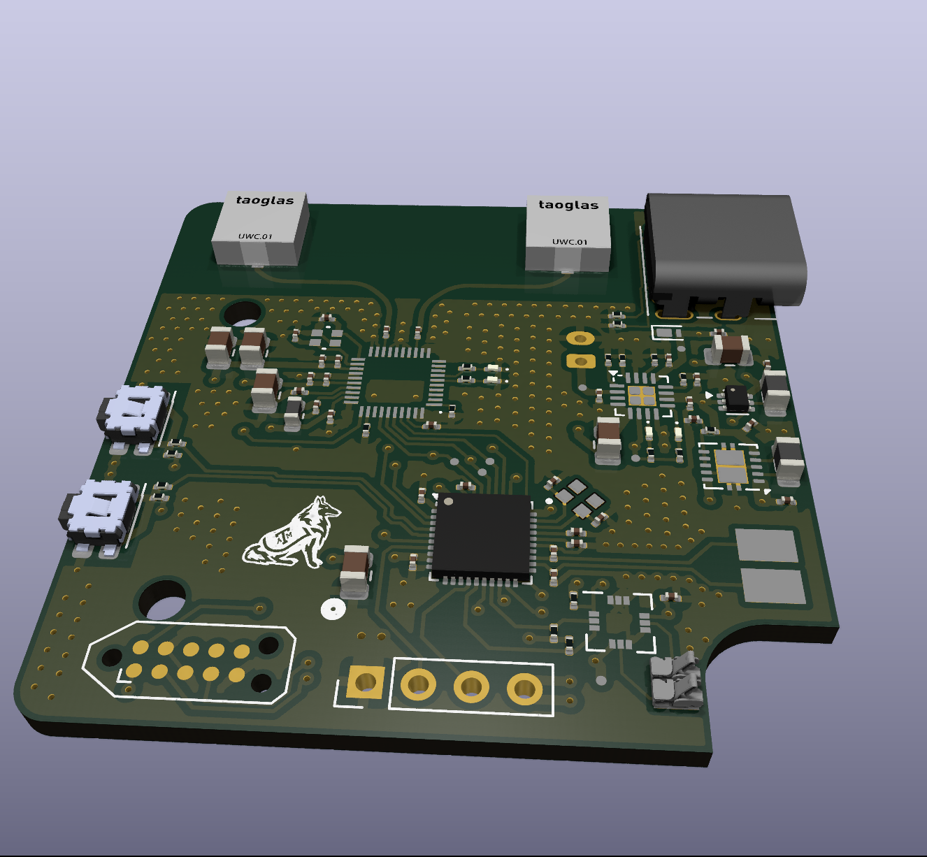
We were able to order the pcbs and the components pretty quickly after the completition of the pcb layout. What we didn't expect was the amount of time it would take to receive them. JLCPCB handled our plain PCB fabrication. The total process to recive the boards took around two weeks (incl. shipping). We ordered assemebled boards from PCBway at the same time and those took over a month. By the time they actually came in, it was the day of our final showcase and we were unable to use them. This wasn't the fault of the fabricators but rather our first and most major mistake.
Since we had so many components, we had unforentuely ran into circumstances where values or sizing were incorrectly copied or had changed and had not been properly updated. Also since kicad and other similar options don't offer grat collaboration features we were stuck with one person working on it at a time. With PCBWay we were able to get the issues corrected, but each time there was an issue we would have to respond by email and wait a full buisness day for a response (due to the time difference). If we were to do this project again ordering early and ensuring that the product list was infallable would have fixed our biggest issues.
Since the assembled boards arrived too late, we were forced to hand assemble one of our own. I had soldered before, but this was microsoldering due to our size constraints. Most of our components were barely visible, let alone easily soldered. This was also the first time I had tried to do chip pad soldering. The entire assembly process took me around three weeks just working around my schedule.
Running into issues and lessons learned
I had headlined the hardware design process for our board and was frankly, exhausted. We had previously split into two teams (hardware and software) and we were able to hand of the completed chip to the software team. Here we ran into other issues. While the written software worked on the development board (a manufacter produced general purpose pcb that uses the same SoC) the development board was not able to program our chip. The unfortunate case was we no longer had the time to undergo in depth debugging. We were able to talk to the company briefly, but we could not come up with a solution before the final presentation. Our primary takeaway was the importance of thorough upfront planning to prevent late-stage integration issues. We also recived indirect feedback at showcase. If you are going to a showcase like ours where judges pick their stops soley based on the name, ensure you don't name it any "tinder" like name. Several judges implied that they had been hesistant to stop out of fear we were a tinder clone.
Future plans
Our group will not personally return to this project. Hopefully, groups in the future might pick it up and develop their own version of it. What we ended up creating, after all, is a extensible development platform. We personally envisioned very simply adding functionality like health tracking, accelerometers for movement, or using it aerospace projects for swarm managment.
If you would like to use the design or are a future capstone group, please don't hesitate to contact me -- I would love to see more life be brought to this project.